|
Capabilities |
|
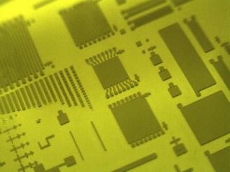
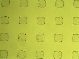
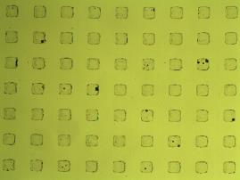
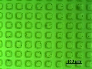
Some examples of our microfabrication capabilities such as lithography with 20 and 2 micrometer resolution, SU-8 development, plasma etching, PDMS molding….etc. This is not a complete list. · Lithography with a resolution of 20 µm using 2.8 µm thick photoresist (Microposit 1828) and high resolution (3000 dpi) transparencies.
|
|
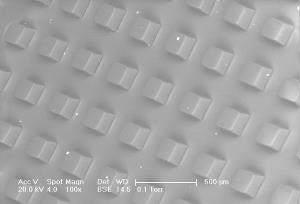
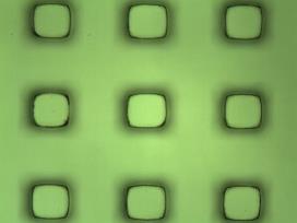
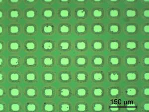
30 µm minimum photoresist patterns achieved using a 3000 dpi transparency mask in our lab. |

|
· Polymer Diode, Transistor and Light Emitting Diode Fabrication: Using semiconducting polymers, ITO and a metal layer, polymer diodes, transistors and LED on flexible PET substrate and glass substrate has been fabricated. |
|
2.8 µm thick photoresist pattern on Silicon as a master. |
|
100 µm thick SU-8 pattern on Silicon as a master. |
|
PDMS mold formed from the master on the left. |
|
· SU-8 Microfabrication: Using SU-8 2100, 100 µm thick SU-8 micro patterns are achieved. |
|
· Electroplating Ni/Fe films · Patterning thin Ni/Cu electrons on PVDF film: 28 µm thick polarized PVDF film, which is piezoelectric, has 100 angstrom Ni/Cu layer on both sides. Metal films on both sides of the PVDF film has been patterned. |
|
· Patterning ITO coated PET: A transparent conducting material, ITO, has been patterned on flexible and transparent substrate, PET. |
|
PMMA patterns as a result of soft lithography using the PDMS stamps mentioned above. |
|
· PDMS (polydimethylsiloxane) Molding and Soft Lithography: Using photoresist and SU-8 patterns as master, PDMS molds are formed to be used in soft lithography or other applications. |
|
2.8 µm thick photoresist pattern on Silicon as a master. |
|
PDMS mold formed from the master on the left. |
|
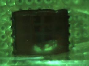
No voltage is applied. |
|
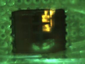
DC voltage is applied. Two orange LEDS are on. |
|
· Cr, Au, Ti, Al (Chromium, Gold, Titanium, Aluminum) Thin Film deposition (Thermal evaporation) and wet etching: Using our NanoVak thermal evaporator we can routinely deposit these thin films with a deposition rate of 1-10 Angstrom/s. Since we have two sources, we can do consecutive film depositions without breaking vacuum. |
|
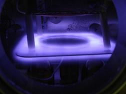
· Oxygen Plasma Cleaning and Surface Treatment: Using our NanoVak thermal evaporator and an oxygen gas, we can routinely create oxygen plasma in our high vacuum chamber at different pressures and voltages. On the right picture, a generated oxygen plasma inside the chamber can be seen. |
|
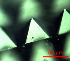
· Anisotropic Etching of Silicon with KOH: Using a heated solution of KOH, anisotropic etching of silicon have been achieved. |
|
Anisotropically etched silicon wells shaped as inverted pyramids. |
|
PDMS pyramids formed using the silicon wells on the left. |
|
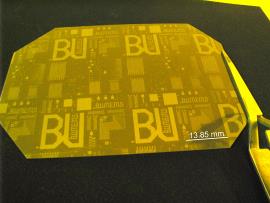
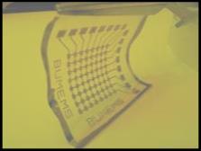
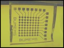
BogazIcI UnIversIty MIcro Electro MechanIcal Systems (BUMEMS) |