


|
BogazIcI UnIversIty MIcro Electro MechanIcal Systems (BUMEMS) |


|
Shining polymer LED examples |


|
Welcome to the website of the Bogazici University Micro Electro Mechanical Systems (BUMEMS) laboratory. This laboratory is dedicated to research on MEMS, Wireless and Batteryless Sensors and Actuators, Circuits, MEMS-Circuit integration and polymer microfabrication including organic / polymer electronics and microfluidics. It was founded on September 2005 by Prof. Senol Mutlu at the Department of Electrical and Electronics Engineering. |


|
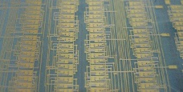
Detailed view of the fabricated Polymer IC showing metal layers and vias. |
|
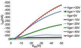
Ids-Vds Curve of a fabricated PFET |
|
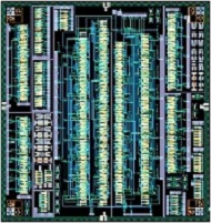
Layout of a Polymer Digital IC designed using IC tools |
|
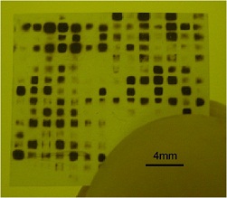
Picture of a Fabricated Polymer IC |
|
Examples of Our Polymer / Organic Electronics |
|
Examples of Polymer Light Emitting Diodes |
|
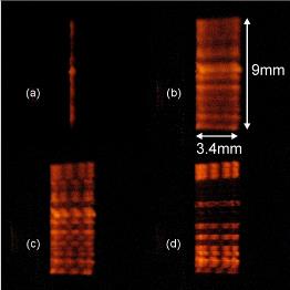
Successfully generated MEMS display image examples (2009). (a) no actuation and no modulation (b) actuated but no modulation (c) PLED array is modulated to give a checker board image (d) pattern obtained by selectively turning off several PLEDs. (In collaboration with A.D. Yalcinkaya) |
|
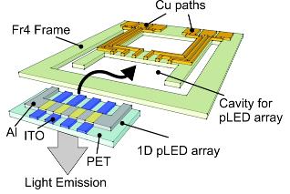
For the first time, a fire resistant 4 (FR4) actuator suspended with two springs at the anchoring regions and an array of polymer light emitting diodes (PLEDs) placed on the actuator surface are integrated to form a polymer display. Slow-scan movement of the MEMS actuator and the electronic modulation of the LEDs form virtual pixels and thus generate a two-dimensional image. (In collaboration with A.D. Yalcinkaya)
|
|
Examples of Polymer LED Integrated Polymer Scanner |
|
Microheater Matrix Using Polymer Semiconductor Diodes for Thermal Patterning |
|
Thermal pictures of the 16x16 heater matrix taken by an infrared thermal imaging camera. An area consisting of 4x4 heaters are selected and current densities of a) 0, b) 1, c) 2 and d) 3 mA/mm2 are applied. |
|
Thermal patterns generated by the heater matrix on a thermal paper. |
|
For the first time, polymer semiconductor diode matrix is used for thermal patterning. The system can generate thousands of individually addressable hotplates (diodes) to generate thermal gradients or hot spots for chemical and biological reactions. |
|
Generated patterns on the wall using steel scanner (In collaboration with A.D. Yalcinkaya) |
|
Experimental Setup for the steel scanner (In collaboration with A.D. Yalcinkaya) |
|
Examples of Steel Micro Scanners |
|
Fabricated two-axis steel scanner |
|
Realization of Charge Pump Circuits Using Polymer Diodes |

|
Schematic representation of a single stage AC to DC charge pump |

|
DC Vout vs. frequency plots for various AC Vin values.
|
|
Polymer diodes made of P3HT are used to build an AC to DC charge pump circuit. Circuit’s frequency response and charge-up time is measured. |
|
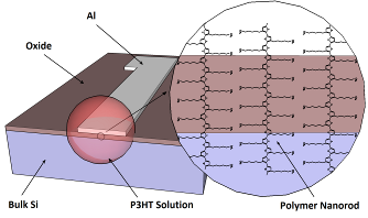
Solution State Diode Using Semiconductor Polymer Nanorods with Nanogap Electrodes |


|
Certain semiconductor polymers such as P3HT stay as nanorods inside its solvent. These nanorods are used inside its solution with electrodes, which have nanogaps that are longer than the lengths of the nanorods. This forms a diode with a higher mobility since intra-chain conduction dominates instead of hopping enabled inter-chain conduction. |
|
Demonstration of the device. P3HT nanorods in solution forms a diode between electrodes with nanogap |
|
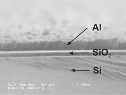
SEM picture of Al and Si electrodes with nanogap formed by SiO2. |
|
Setup for the experiments. Dipping the electrodes with nanogap into the solution is enough to form a diode. |
|
I-V curve of a diode is seen only when the electrodes with nanogap are dipped into the polymer solution, not in air or in solvent. |


|
Planar Water Gated Organic Field Effect Transistor Using Hydrophilic Polythiophene for Improved Digital Inverters |
|
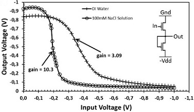
Operation of a planar water gated OFET is demonstrated for the first time. P3HT is functionalized with poly(ethylene glycol) to make it more hydrophilic. Double layer gate capacitance increases 1.8 times with hydrophilic polythiophene. Transconductance triples by using 100 mM NaCl solution instead of DI water. Inverters are build with a gain of 10 V/V using OFETs with best transconductances. |
|
Hydrophilic P3HT-co-P3PEGT |
|
Planar Water Gated OFET Structure |
|
Photograph of a fabricated planer water-gated OFET |
|
Molecular structures of P3HT-co-P3PEGT |
|
Voltage transfer characteristics of fabricated inverter utilizing P3HT-co-P3PEGT for different electrolyte solutions |
|
Hexyl side chain |
|
Polyethylene glycol (PEG) side chain |

|
Light Emitting Diode as a Power Supply for Wireless and Batteryless Microsystems |
|
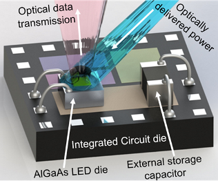
A light emitting diode (LED) is used as a power supply to a wireless and batteryless microsystem for the first time. Three different application specific integrated circuits (ASIC) are designed, manufactured and tested for this purpose. The microsystem can be powered optically through LED and transmit its data optically using the same LED. Related work is published in IEEE JMEMS and Transactions on Circuits and Systems I. |
|
Photo of an implemented microsystem |


|
Optically received data from 10 cm, using a transimpedance amplifier based photodetector circuit built in-house. |
|
Conceptual representation of the optically powered and optically transmitting microsystem using a single light emitting diode. |
|
We made a presentation at ISSCC 2016: ISSCC (International Solid-State Circuits Conference) is the flagship conference of the IEEE Solid-State Circuits Society. The semiconductor industry generated about $290 billion in sales in 2012. ISSCC is one of the premier technical forum for presenting advances in solid-state circuits and systems. Around 3000 people from academia and industry attend ISSCC. Corporate attendees from the semiconductor and system industries typically represent around 60% of the attendees. I. Haydaroglu, M. Ozgun, Senol Mutlu, Presentation, 2016 International Solid State Circuits Conferene (ISSCC) Student Research Preview session (Student work in progress), Jan. 31-Feb. 4, San Francisco, CA. We designed and tested a wireless and batteryless IC that uses a single light emitting diode (LED) to efficiently harvest optical energy and transmit data concurrently. LED voltage is sufficient to sustain continous opetation at 6 uW. A switched capacitor boosting driver pulses current through the LED to transmit data with 1 nJ/bit, recorded by an on-chip temperature sensor. This can be received externally from a 10 cm distance using an external photodetector with transimpedance amplifier. |
|
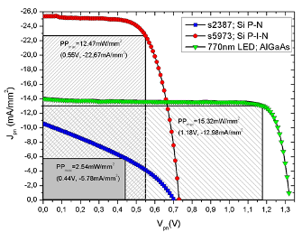
Current density vs voltage plots for commercial silicon PIN diode, 770 nm LED, and silicon photodiode under 68 mW/mm2 (120 mW power with a spot size of 1,5 mm diameter) 680 nm laser illumination. Corrected for effective device area; 1.2mm2 for s2386, 0.12mm2 for s5973 and 0.1mm2 for LED. |
|
HOME |
|
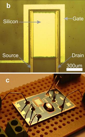
Published in Nature.com/Scientific Reports: Water-Gated Field Effect Transistor (WG-FET) Using 16-nm-Thick Mono-Si Film |
|
A micrograph of a fabricated WG-FET device with planar-gate topology and Experimental setup for current-voltage measurements. |

|
An illustration of a WG-FET device with source-drain electrode insulation |
|
IDS-VDS measurement results for probe gate setup without source-drain electrode insulation. VGS is swept from 0 V to -1 V. |
|
We introduced a novel water-gated field effect transistor (WG-FET) which uses 16-nm-thick mono-Si film as active layer. WG-FET devices use electrical double layer (EDL) as gate insulator and operate under 1 V without causing any electrochemical reactions. Best on/off ratios are measured for probe-gate devices as 23,000 A/A and 85,000 A/A with insulated and uninsulated source-drain electrodes, respectively. |


|
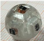
Published in Advanced Science: Magnetic Resonance Imaging-Compatible Optically Powered Miniature Wireless Modular Lorentz Force Actuators |
|
A. (i) Schematic description of a single actuator module with the related physical parameters involved, and (ii) photograph of an experimental actuator module prototype with its components. B. Equivalent electrical circuit diagram of the actuator module. C. Building different actuation mechanisms inside a preclinical MRI scanner (B0 = 7 Tesla) using different number of actuator modules: (i) one wireless module that can bend a flexible cantilever beam, (ii) four wireless modules that can rotate around an axis, and (iii) six wireless modules inside a spherical shell that can rotate around itself and roll on surfaces along B0 direction. |


|
Photograph of the 3D-printed plastic sphere and six actuator modules before and after assembly. |
|
Movie of wireless rotor motion inside 7 Tesla MRI scanner |

|
No image artifact of the wireless rotor when off |
|
Movie of the spherical roller on a 0.25 Tesla permanent magnet with IR light radiation as it spins and hits the walls of the plastic container. |


|
Instantenous turning-on of 146 LEDs connected in series with a single foot step on the triboelectric energy harvester |

|
Microphotograph of the integrated circuit |
|
System architecture of the triboelectric energy harvesting integrated circuit. |
|
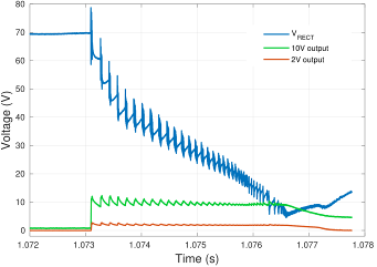
Test results of the integrated circuit |
|
Congratulations to Ismail Kara on earning his Ph.D. and publication in IEEE Transactions on Circuits and Systems I: Regular Papers: A 70-to-2 V Triboelectric Energy Harvesting System Utilizing Parallel-SSHI Rectifier and DC-DC Converters |
