|
Research |
|
The research interests of this laboratory can be summarized as below. MEMS, sensors and actuators, circuits, MEMS-circuit integration, energy harvesting and microfluidics are the core interests of this lab. · Micro ElectroMechanical Systems (MEMS) · Integrated Wireless and Batteryless Sensors and Actuators · Energy Harvesting · Microfluidics and BioMEMs · Organic Electronics and Polymer Light Emitting Diodes · Polymer Thin Film Microfabrication · Micropumps and Microvalves · Electrochemical Etching and Deposition for Nano/Micro Patterning
|
|
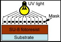
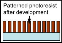
Some old examples of research activities are given below. This is not a complete list. SU-8 and PDMS Microfabrication SU-8 is a commonly used negative photoresist in MEMS. Its popularity has increased recently in this area because SU-8 can be spin-coated, is chemically stable, once developed it does not react with other chemicals, can have a high aspect ratio (about 10) and its thickness can be between 1 and 300 µm. Its fabrication process is summarized below, in Figure 1. |
|
Figure 1. SU-8 fabrication method that will be followed at the BUMEMS lab. |
|
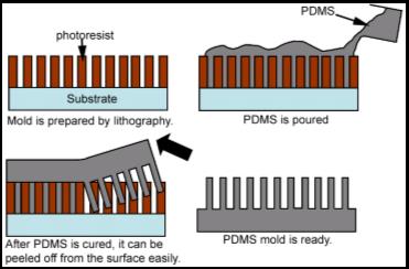
One important difference in our efforts is that the lithography steps will use simple alignment apparatus instead of very expensive contact aligners and high resolution transparencies (5000 dot per inch) as masks instead of chrome coated glass masks, which are expensive and need too much time for development. Using this method, 20 µm pattern and alignment resolution can be achieved. After this development, polydimethylsiloxane (PDMS) molds will be fabricated out of SU-8 molds as summarized in Figure 2. PDMS is very soft and flexible so it can be peeled of from surfaces very easily. |
|
Figure 2. Fabrication of PDMS molds out of SU-8 molds. |
|
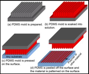
Soft-lithography with PDMS Molds Using fabricated PDMS molds soft-lithography can be achieved. This term is used for a simple stamping method. The PDMS is soaked into the solution with the desired material that needs to be patterned. Then the PDMS mold is stamped on the surface and that material gets patterned as shown in Figure 3. |
|
Figure 3. Soft lithography method is used to pattern a polymer or other material. |
|
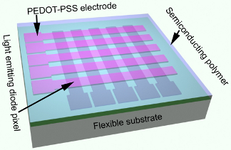
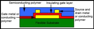
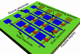
Conducting and Semi-conducting Polymer Microfabrication Conducting polymers like Poly(3,4-ethylenedioxythiophene) poly(styrenesulfonate) (PEDOT-PSS) and semiconducting polymers like pentacene, poly(9,9-dioctylfluoreneco-bithiophene) (F8T2), poly(2-methoxy, 5-(2’-ethyl-hexyloxy)-1,4-phenylene vinylene) (MEH-PPV), [6,6]-phenyl-C61-butyric acid methyl ester (PCBM) ve poly(3-(2-butyloxy-5-octylphenyl)thiophene (PBOPT) can be patterned on any substrates like flexible and transparent plastics using spin-coating, soft lithography and even ink-jet printing. Then, flexible displays with polymer light emitting diodes (LED) and simple transistors and electronic circuits can be fabricated on flexible substrates. Schematics of these devices are shown in the Figure 4 and 5. |

|
Figure 4. Flexible display with polymer LEDs. LED cross-section on the left, and the top view of the display on the right. |
|
Figure 5. Polymer transistor. cross-section on the left, and the top view of the transistor matrix on the right. |
|
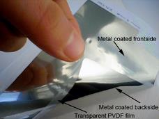
Piezoelectric Polymer Microfabrication Piezoelectric polymer, poly VinyliDene Fluoride (PVDF), is a very versatile polymer. It is flexible, transparent and has piezoelectric property. Also it is chemically inert. Furthermore, it is available commercially as a thin film with a desired thickness and its both sides can be coated with metal. One example of a purchased PVDF film with its both sides coated with metal is shown in Figure 6. Tactile sensors and tactile imagers can be developed by microfabricating this film. |
|
Figure 6. Picture of a piezoelectric polymer (PVDF) film |
|
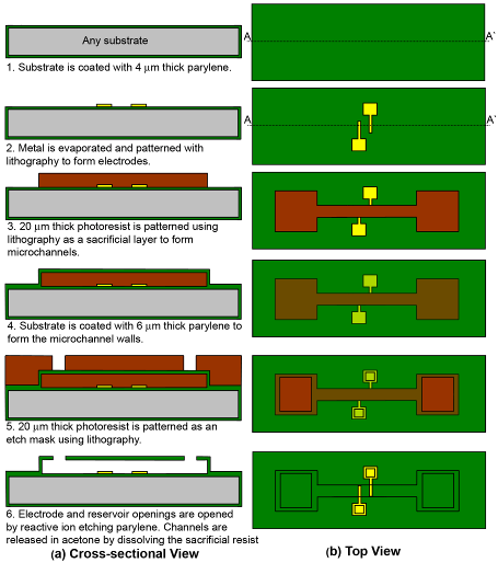
Parylene Micfabrication Parylene is commonly used in MEMS now because its film is conformal, pin-hole free, deposited at room temperature, has lower outgassing and lower permeability to liquids and gasses compared to other polymers, has high optical clarity and no background fluorescence, is a good electrical insulator, chemically inert and biocompatible. However, its most important property is that it can be easily integrated with CMOS. It can be used to integrate multilevels of microchannels, electrodes and microheaters together. |
|
Figure 7. Parylene microfabrication method for the integration of microchannels and electrodes. |
|
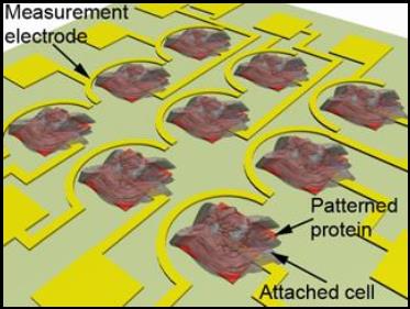
Parylene can also be used as a mechanical material to fabricate surface micromachined beams, diaphragms and cantilevers for applications that require low Young’s modulus. Therefore, parylene technology can be used as a platform to integrate CMOS and electrodes, heaters, microchannels, cantilevers, beams and diaphragms. Parylene microfabrication method to integrate microchannels with electrodes is shown in Figure 7. Protein and Cell Patterning Using soft lithography or gold-alkanethiol interaction, proteins can be patterned on glass or silicon surfaces. If motor proteins like kinesin is patterned on the surface, their interaction with microtubules can be used to transport molecules from one part of the chip to the other part. If the patterned proteins are extra cellular matrix protein like fibronectin, vitronectin and laminin, then cells can attach themselves to these proteins. Therefore, by patterning proteins on the surface and then culturing cells on it, cells will attach themselves to only protein patterns and therefore, they will be patterned on the surface as shown in Figure 8. This way, muscle and nerve cells can be patterned on a surface and their interaction can be analyzed electrochemically using micromachined electrodes or using other methods. |
|
Figure 8. Cells attached on patterned proteins on a surface of a substrate with patterned measurement electrodes. |
|
BogazIcI UnIversIty MIcro Electro MechanIcal Systems (BUMEMS) |